


NVIDIA Corporation and the Volta Process Mystery
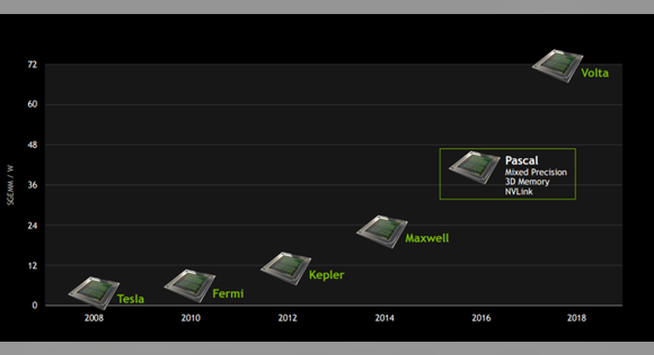
Image source: NVIDIA.
At graphics specialist NVIDIA's most recent financial analyst day, one analyst asked CEO Jen-Hsun Huang the following question:
Now, since then, NVIDIA has announced at least two Pascal-based products built on the same Taiwan Semiconductor Manufacturing Co. 16-nanometer manufacturing technology as the data-center-oriented Tesla P100 that was announced at the analyst day. Additionally, rumors suggest that additional members of the Pascal family, also built on the 16-nanometer node, will be out fairly shortly.
Despite what we already know about the consumer Pascal cards, I still believe the answer is quite interesting and potentially illuminating. Let's take a look.
16-nanometer isn't going to be a short node
"We're going to use 16-nanometer for some time because 16-nanometer is a really good process, it's a good node" Huang began. "There's no immediate reason why we'd jump to 10 [nanometer] or 7 [nanometer]."
That being said, Huang did say that NVIDIA is doing "test chips on 10 [nanometer] and 7 [nanometer]" and that "when the appropriate time comes, we'll absolutely go [to these new nodes]."
What do these comments suggest?
The reason that I'm interested in what Huang had to say here is that I am trying to puzzle out what manufacturing technology NVIDIA will use for its next-generation graphics processor family based on the Volta architecture.
NVIDIA expects a big boost in power efficiency in going from Pascal to Volta. Image source: NVIDIA.
Note that Summit supercomputer at the Oak Ridge National Laboratory is expected to come online in 2017. This supercomputer will use Volta, so this means that the GV100 chip (NVIDIA's high-performance computing-oriented Volta chip) will need to ship in 2017.
In order for the chip to be production-ready for late 2017 deployments, it should be taping out right around now as it's often a year from initial tape-out to mass production.
If, as of Huang's comments back in early April, NVIDIA was still working on test chips, then this could mean that the company is a ways off from qualifying a very high-performance data-center-oriented process on 10-nanometer (or 7-nanometer) for production.
Perhaps Volta is a 16-nanometer product family after all?
At this point, it's not clear to me what chip manufacturing technology the upcoming Volta will use. On one hand, it would seem that the company will need to transition to a new manufacturing technology in order to dramatically improve performance from Pascal, particularly for data centers.
After all, the GP100 chip that NVIDIA recently announced measures in at 601 square millimeters and is rated at a 300 watt thermal design power. NVIDIA won't have a lot of room to increase the size of the chip since the GP100 is probably close to -- if not at -- the physical limit of what can be manufactured on Taiwan Semi's 16-nanometer process.
On the other hand, the comments around "test chips" on 10-nanometer and 7-nanometer suggest that Volta could very well wind up being a 16-nanometer part. In that case, NVIDIA will need to make very significant strides in both architectural area and power efficiency to be able to achieve what it wants to with Volta.
The article NVIDIA Corporation and the Volta Process Mystery originally appeared on Fool.com.
Ashraf Eassa has no position in any stocks mentioned. The Motley Fool owns shares of and recommends NVIDIA. Try any of our Foolish newsletter services free for 30 days. We Fools may not all hold the same opinions, but we all believe that considering a diverse range of insights makes us better investors. The Motley Fool has a disclosure policy.
Copyright 1995 - 2016 The Motley Fool, LLC. All rights reserved. The Motley Fool has a disclosure policy.